E-beam Lithography
Overview
Electron beam lithography (often abbreviated as e-beam lithography) is the practice of scanning a focused beam of electrons to draw custom shapes on a surface covered with an electron-sensitive film called a resist. The electron beam changes the solubility of the resist, enabling selective removal of either exposed or non-exposed regions of the resist by immersing it in a suitable developer solution. This technique is used in microfabrication to create very small structures in the nanometer range.


History
The development of e-beam lithography was a significant milestone in the field of nanotechnology. The technique was first developed in the 1960s as a result of advancements in electron microscopy. It was quickly recognized as a powerful tool for the fabrication of micro- and nanostructures, and has since been used extensively in the research and development of semiconductor devices, nanophotonics, and nanoelectronics.
Principles of Operation
E-beam lithography operates on the principle of the interaction between a focused beam of high-energy electrons and a resist-covered surface. The energy of the electrons is sufficient to break the chemical bonds in the resist, changing its solubility. The resist can be either positive or negative. In a positive resist, the exposed areas become more soluble and can be removed by the developer solution, leaving behind the unexposed areas. In a negative resist, the exposed areas become less soluble and remain after development, while the unexposed areas are removed.
Equipment
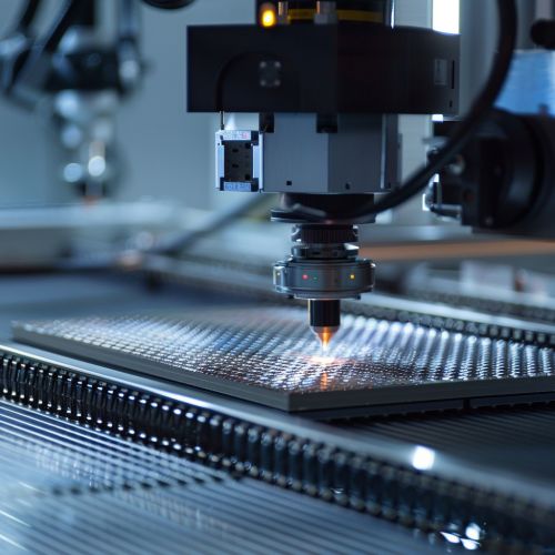
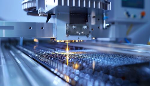
The key components of an e-beam lithography system include an electron gun for generating the electron beam, a system for focusing and deflecting the beam, a vacuum chamber to maintain a clean environment, a stage for holding and moving the resist-covered substrate, and a computer system for controlling the beam and stage movements.
Applications
E-beam lithography is used in a variety of applications, including the fabrication of integrated circuits, microelectromechanical systems (MEMS), nanofluidic devices, and photonic crystals. It is also used in the creation of quantum dots, nanowires, and other nanostructures.
Advantages and Disadvantages
E-beam lithography offers several advantages over other lithographic techniques. It can create structures with dimensions in the nanometer range, and it allows for the creation of custom patterns without the need for a mask. However, it also has some disadvantages. The process is slow, as each point in the pattern must be individually written by the electron beam. It is also expensive, due to the high cost of the equipment and the need for a cleanroom environment.
