Photolithography
Introduction
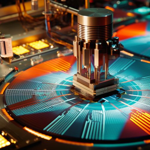
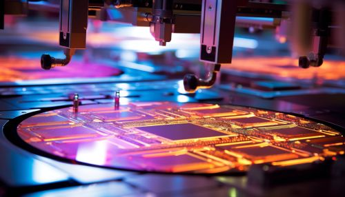
Photolithography, also known as optical lithography or UV lithography, is a process used in microelectronics to pattern parts of a thin film or the bulk of a substrate. It uses light to transfer a geometric pattern from a photomask to a light-sensitive chemical "photoresist", or simply "resist," on the substrate. A series of chemical treatments then either engraves the exposure pattern into the material or enables deposition of a new material in the desired pattern upon the material underneath the photoresist.
History
Photolithography originated in the 19th century with the use of light to transfer geometric patterns from a photomask to a light-sensitive chemical photoresist on the substrate. The process has been refined and advanced over the years, with significant developments occurring in the mid-20th century with the advent of the semiconductor industry.
Process
The process begins with a substrate, typically silicon, which is cleaned and coated with a layer of photoresist. The photoresist is a light-sensitive material that changes its properties when exposed to ultraviolet light. The substrate and photoresist are then placed beneath a photomask, which contains the desired pattern.


The photomask is aligned with the substrate, and ultraviolet light is shone onto the surface. The light passes through the clear areas of the photomask, exposing the photoresist underneath. The exposed areas of the photoresist undergo a chemical reaction, changing their properties and making them soluble in a developer solution.
The substrate is then immersed in the developer solution, which removes the exposed photoresist, leaving behind the unexposed photoresist and revealing the pattern. The exposed areas of the substrate can then be etched or have material deposited on them, depending on the desired outcome.
Applications
Photolithography is used extensively in the semiconductor industry to manufacture integrated circuits (ICs). It is also used in the fabrication of microelectromechanical systems (MEMS), microsystems technology (MST), and nanotechnology. Other applications include the manufacture of flat panel displays, thin-film magnetic heads, and micro-optical components.
Limitations and challenges
One of the main challenges in photolithography is the resolution, or the smallest feature that can be created on the substrate. The resolution is limited by the wavelength of the light used in the process, with shorter wavelengths allowing for smaller features. This is known as the diffraction limit.
Another challenge is the depth of focus, which is the range in which the photoresist layer can be accurately patterned. If the depth of focus is too shallow, it can lead to uneven patterning across the substrate.
Future developments
As the demand for smaller and more complex devices continues to grow, new methods of photolithography are being developed to overcome the limitations of traditional photolithography. These include extreme ultraviolet lithography (EUVL), immersion lithography, and multiple patterning techniques.
