Semiconductor device fabrication
Introduction
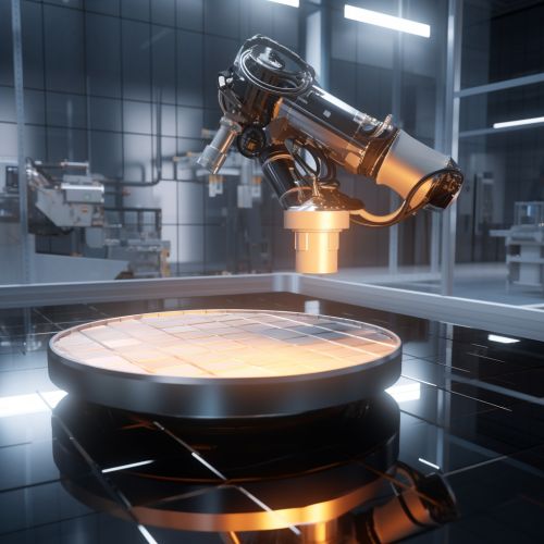
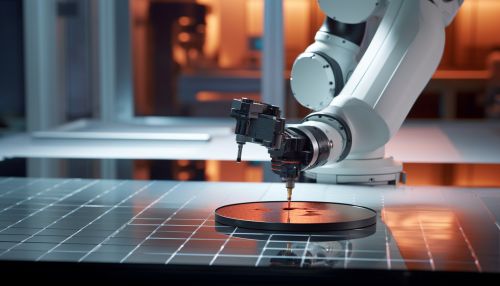
Semiconductor device fabrication is the process used to create the integrated circuits that are present in everyday electrical and electronic devices. It is a multiple-step sequence of photolithographic and chemical processing steps during which electronic circuits are gradually created on a wafer made of pure semiconducting material. Silicon is almost always used, but various compound semiconductors are used for specialized applications.
Silicon Wafer Preparation
The process begins with the creation of a silicon wafer. This is done by first converting raw silicon into a single crystal substrate. The silicon is first purified via the Czochralski process. In this process, a silicon crystal 'seed' is put in a bath of molten silicon. The seed is then pulled slowly upwards and rotated simultaneously. This results in a large round cylinder, or 'boule', of pure silicon. The boule is then sliced into wafers, approximately 0.75 mm thick. These wafers are then polished to a mirror finish before being cleaned.


Oxidation
The next step in the process is the oxidation of the silicon wafer. This is done in a high temperature furnace, where the wafer is heated to approximately 1,000 degrees Celsius in an oxygen atmosphere. The oxygen reacts with the silicon to form silicon dioxide, which grows as a layer on the silicon wafer. This silicon dioxide layer can be grown to a thickness that can be controlled to within a few angstroms.
Photolithography
The next step in the process is photolithography. This involves coating the wafer with a light-sensitive material called photoresist. The wafer is then exposed to a pattern of intense light, which causes the photoresist to harden where it is exposed. The unexposed photoresist is then etched away, leaving a pattern of photoresist on the silicon dioxide.
Etching
The next step in the process is etching. The most common method of etching is called plasma etching. In this process, a gas containing a reactive species is introduced into a plasma reactor. The plasma is created by applying a strong electromagnetic field to the gas, which causes the gas to ionize and become a plasma. The plasma then reacts with the silicon dioxide and the photoresist, etching away the exposed silicon dioxide and leaving behind the patterned photoresist.
Doping
The next step in the process is doping. This is the process of adding impurities to the silicon to change its electrical properties. There are two types of doping: n-type, where the impurity atoms are donors, and p-type, where the impurity atoms are acceptors. The doping process is done by ion implantation, where a beam of ions is fired at the silicon wafer. The ions penetrate the silicon and change its electrical properties.
Metallization
The final step in the process is metallization. This is the process of depositing a thin layer of metal onto the silicon wafer to form the electrical connections between the different parts of the integrated circuit. The most common method of metallization is sputtering, where a target made of the metal to be deposited is bombarded with ions. The impact of the ions causes atoms of the metal to be ejected from the target and deposited onto the silicon wafer.
Conclusion
Semiconductor device fabrication is a complex, multi-step process that requires a high degree of precision and control. Despite the complexity of the process, it has been refined and optimized over many decades, resulting in the ability to produce integrated circuits with billions of transistors on a single silicon wafer.
