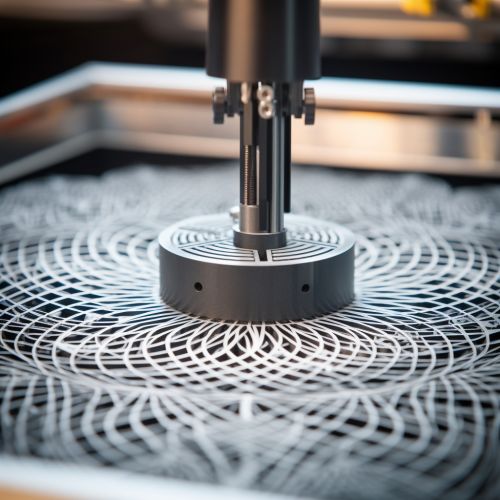
Nanoimprint Lithography
Introduction
Nanoimprint lithography (lithography) is a method of fabricating nanometer scale patterns. It is a simple nanopatterning process with the potential for high throughput, which is considered an alternative to traditional photolithography. The process involves imprinting a pattern onto a substrate by mechanical deformation and filling the resulting trenches with a second material. The imprinting process can be performed at room temperature and does not require expensive equipment or high energy radiation sources.


History
The concept of nanoimprint lithography was first proposed by Prof. Stephen Y. Chou and his group at Princeton University in 1995. The process was initially referred to as "LRL" (Lithographically Induced Self-Construction), and later renamed to "Nanoimprint Lithography". The technique was developed as a cost-effective and high-resolution alternative to traditional lithographic methods such as electron beam lithography (EBL) or photolithography.
Process
Nanoimprint lithography involves the following steps:
- Application of a low viscosity resist to the substrate. The resist is typically a monomer or polymer formulation that is cured by heat or UV light.
- The resist is brought into contact with a template (or mold) which has the desired pattern etched into its surface.
- The resist is cured, causing it to harden and take on the pattern of the template.
- The template is removed, leaving the patterned resist on the substrate.
- The patterned resist can then be used as a mask for etching or additive processes to create the final patterned structure on the substrate.
The process can be performed with either a single step imprinting and curing process (hot embossing), or a two-step process where the resist is first imprinted and then cured (UV-NIL).
Types of Nanoimprint Lithography
There are several types of nanoimprint lithography, including thermal nanoimprint lithography, UV nanoimprint lithography, and soft lithography.
- Thermal Nanoimprint Lithography ###
In thermal nanoimprint lithography (T-NIL), the resist is heated above its glass transition temperature (Tg) before the mold is pressed into the resist. After the resist cools and hardens, the mold is removed.
- UV Nanoimprint Lithography ###
In UV nanoimprint lithography (UV-NIL), a low viscosity, UV-curable resist is used. The mold is pressed into the resist and then exposed to UV light to cure and harden the resist. The mold is then removed.
- Soft Lithography ###
Soft lithography is a type of nanoimprint lithography that uses elastomeric molds, typically made of polydimethylsiloxane (PDMS). This allows for the creation of flexible and stretchable structures.
Applications
Nanoimprint lithography has been used in a variety of applications, including the fabrication of high-density data storage devices, photonic crystals, light-emitting diodes (LEDs), and biological and chemical sensors. It has also been used in the fabrication of nanoscale devices for electronics, optoelectronics, and photonics.
Advantages and Disadvantages
The main advantages of nanoimprint lithography include its high resolution, low cost, and high throughput. It is capable of patterning features down to the nanometer scale, and can do so over large areas, making it suitable for mass production. It also does not require the use of expensive equipment or high energy radiation sources, making it a cost-effective method of nanopatterning.
However, there are also some disadvantages to nanoimprint lithography. These include the potential for defects caused by dust particles or other contaminants, the need for precise alignment of the mold and substrate, and the potential for damage to the mold during the imprinting process.
Future Directions
Current research in nanoimprint lithography is focused on improving the process and expanding its applications. This includes the development of new resists and molds, the use of self-assembled monolayers (SAMs) to reduce adhesion between the mold and resist, and the use of directed self-assembly (DSA) to guide the formation of patterns.
