Lithography (microfabrication)
Overview
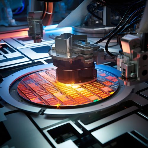
Lithography in the field of microfabrication is a process used to transfer a pattern in the photomask to the surface of a silicon wafer. The process is named after the traditional method of lithography used in printing, where a pattern is transferred from a photomask to paper. However, in microfabrication, the process is used to create intricate patterns on a silicon wafer, which are then used to build microchips and other microdevices.
History
The use of lithography in microfabrication began in the 1960s with the development of the integrated circuit. The first microfabrication processes used photolithography, a process that uses light to transfer a pattern from a photomask to a light-sensitive chemical, or photoresist, on the silicon wafer. This process allowed for the creation of intricate patterns on the silicon wafer, which were then used to build the integrated circuits.
Process
The process of lithography in microfabrication involves several steps. First, the silicon wafer is cleaned to remove any dust or other contaminants. Next, a layer of photoresist is applied to the wafer. The photoresist is a light-sensitive chemical that changes its properties when exposed to light.
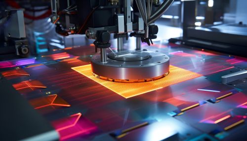
The photomask, which contains the pattern to be transferred to the wafer, is then aligned with the wafer. The wafer and photomask are then exposed to light, which causes the photoresist to change its properties in the areas where the light hits it. The unexposed areas of the photoresist remain unchanged.
After the exposure, the wafer is developed, which removes the exposed or unexposed areas of the photoresist, depending on the type of photoresist used. This leaves behind a pattern of photoresist on the wafer.
The wafer is then etched, which removes the areas of the silicon wafer that are not covered by the photoresist. This leaves behind a pattern of silicon that matches the pattern on the photomask.
Finally, the remaining photoresist is removed, leaving behind the patterned silicon wafer.
Types of Lithography
There are several types of lithography used in microfabrication, each with its own advantages and disadvantages.
Photolithography
Photolithography is the most common type of lithography used in microfabrication. It uses light to transfer a pattern from a photomask to a photoresist on a silicon wafer. The main advantage of photolithography is its ability to create intricate patterns on a silicon wafer. However, it is limited by the wavelength of the light used, which determines the smallest feature size that can be created.
E-beam Lithography
E-beam lithography is a type of lithography that uses a focused beam of electrons to create a pattern on a silicon wafer. The main advantage of e-beam lithography is its ability to create very small feature sizes, down to a few nanometers. However, it is a slow process, making it unsuitable for mass production.
X-ray Lithography
X-ray lithography is a type of lithography that uses X-rays to create a pattern on a silicon wafer. The main advantage of X-ray lithography is its ability to create very small feature sizes. However, it requires a complex and expensive X-ray source, making it less commonly used than other types of lithography.
Nanoimprint Lithography
Nanoimprint lithography is a type of lithography that uses a mold to create a pattern on a silicon wafer. The main advantage of nanoimprint lithography is its ability to create very small feature sizes, down to a few nanometers. However, it requires a mold, which can be expensive to create.
Applications
Lithography in microfabrication is used in a variety of applications. It is most commonly used in the production of integrated circuits, where it is used to create the intricate patterns of transistors and other components on a silicon wafer.
In addition to integrated circuits, lithography is also used in the production of microelectromechanical systems (MEMS), such as accelerometers and gyroscopes. These devices are used in a variety of applications, including automotive safety systems, consumer electronics, and medical devices.
Lithography is also used in the production of nanotechnology devices, such as nanowires and nanotubes. These devices have potential applications in a variety of fields, including electronics, medicine, and energy production.


Future Developments
The future of lithography in microfabrication is likely to involve the development of new techniques and technologies to allow for the creation of even smaller feature sizes. One such technology is extreme ultraviolet (EUV) lithography, which uses light with a much shorter wavelength than traditional photolithography. This allows for the creation of feature sizes as small as 5 nanometers.
Another potential future development is the use of directed self-assembly (DSA) techniques, which use the properties of materials to guide their assembly into desired patterns. This could potentially allow for the creation of even smaller feature sizes than are currently possible with existing lithography techniques.
