Electron Microscopy in Materials Science
Introduction
Electron microscopy is a technique that uses a beam of highly energetic electrons to examine objects on a very fine scale. It is a powerful tool in the field of materials science, allowing for the detailed study of the structure, composition, and properties of materials.


History and Development
The development of electron microscopy began in the early 20th century, following the discovery of the electron and the realization of its potential in imaging. The first electron microscope was developed in the 1930s by Ernst Ruska, a German physicist, and Max Knoll. Since then, the technology has evolved significantly, with advancements in resolution, contrast, and imaging techniques.
Principles of Electron Microscopy
Electron microscopy operates under similar principles as light microscopy, but instead of using light, it uses electrons. The shorter wavelength of electrons allows for higher resolution imaging, enabling the visualization of much smaller structures than can be seen with a light microscope.
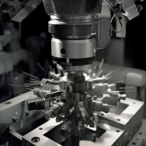
The basic components of an electron microscope include an electron source, electromagnetic lenses, and a detector. The electron source generates a beam of electrons, which is focused by the lenses onto the sample. The interaction of the electrons with the sample generates signals that are detected and used to form an image.
Types of Electron Microscopy
There are several types of electron microscopy, each with its own strengths and applications in materials science.
Transmission Electron Microscopy (TEM)
Transmission electron microscopy (TEM) is a type of electron microscopy that involves passing an electron beam through a thin specimen. This technique allows for the imaging of structures at the atomic level, making it a powerful tool for studying the internal structure of materials.
Scanning Electron Microscopy (SEM)
Scanning electron microscopy (SEM) involves scanning a focused electron beam across the surface of a sample and detecting the resulting signals to form an image. SEM provides detailed images of the surface topography and composition of materials.
Scanning Transmission Electron Microscopy (STEM)
Scanning transmission electron microscopy (STEM) combines the principles of TEM and SEM. In STEM, the electron beam is scanned across the sample, but the electrons are also transmitted through the sample, allowing for the simultaneous collection of surface and internal information.
Applications in Materials Science
Electron microscopy plays a crucial role in materials science, providing detailed insights into the structure and properties of materials.
Structural Analysis
Electron microscopy can reveal the internal structure of materials at the atomic level. This includes information about the arrangement of atoms, the presence of defects, and the size and shape of microscopic features.
Chemical Analysis
Electron microscopy can also provide information about the chemical composition of materials. Techniques such as energy-dispersive X-ray spectroscopy (EDX) and electron energy loss spectroscopy (EELS) can be used to identify the elements present in a sample and their distribution.
Mechanical Property Analysis
The mechanical properties of materials, such as hardness and ductility, are closely related to their structure and composition. Electron microscopy can provide valuable insights into these relationships, aiding in the development of materials with tailored properties.
Future Directions
The field of electron microscopy continues to evolve, with ongoing advancements in technology and technique. Future directions include the development of more powerful detectors, the use of machine learning for image analysis, and the integration of electron microscopy with other analytical techniques.
