Quantum well lasers
Introduction
A quantum well laser is a type of semiconductor laser that utilizes quantum wells to confine carriers in a dimensionally restricted region, thereby enhancing the efficiency and performance of the laser. Quantum well lasers are widely used in various applications, including telecommunications, medical devices, and optical data storage. This article delves into the principles, structure, fabrication, and applications of quantum well lasers, providing a comprehensive understanding of this advanced technology.
Principles of Quantum Well Lasers
Quantum well lasers operate based on the principles of quantum mechanics and semiconductor physics. The key concept is the quantum well, a potential well that confines particles such as electrons and holes in a thin layer, typically a few nanometers thick. This confinement leads to discrete energy levels, which significantly affect the electronic and optical properties of the material.
Quantum Confinement
In a quantum well, the motion of carriers is restricted in one dimension, leading to quantization of energy levels. This phenomenon is known as quantum confinement. The energy levels in a quantum well are determined by the well's thickness and the material's properties. Quantum confinement enhances the interaction between electrons and holes, increasing the probability of radiative recombination, which is essential for laser operation.
Bandgap Engineering
Quantum wells allow for precise control over the bandgap of the semiconductor material. By adjusting the thickness of the quantum well and the composition of the materials used, engineers can tailor the bandgap to achieve desired emission wavelengths. This flexibility is crucial for developing lasers that operate at specific wavelengths required for different applications.
Structure of Quantum Well Lasers
The structure of a quantum well laser typically consists of multiple layers of semiconductor materials with varying compositions and thicknesses. The core components include the quantum well, barrier layers, cladding layers, and the substrate.
Quantum Well and Barrier Layers
The quantum well is sandwiched between barrier layers, which are made of materials with a larger bandgap. These barrier layers confine the carriers within the quantum well. The thickness of the quantum well and the barrier layers is carefully controlled during fabrication to achieve the desired energy levels and optical properties.
Cladding Layers
Cladding layers surround the quantum well and barrier layers, providing optical confinement and guiding the light generated in the quantum well. These layers are typically made of materials with a lower refractive index than the core layers, ensuring that the light remains confined within the active region.
Substrate
The substrate provides mechanical support for the entire structure and plays a crucial role in the epitaxial growth of the layers. Common substrate materials include gallium arsenide (GaAs) and indium phosphide (InP), chosen based on the lattice matching with the active layers.


Fabrication of Quantum Well Lasers
The fabrication of quantum well lasers involves advanced semiconductor processing techniques to achieve the precise control required for quantum well structures.
Molecular Beam Epitaxy (MBE)
Molecular beam epitaxy is a widely used technique for fabricating quantum well lasers. In MBE, beams of atoms or molecules are directed onto a heated substrate in an ultra-high vacuum environment. This method allows for precise control over the thickness and composition of the layers, essential for creating high-quality quantum wells.
Metal-Organic Chemical Vapor Deposition (MOCVD)
MOCVD is another common technique used in the fabrication of quantum well lasers. In this process, metal-organic precursors are decomposed in a chemical reaction to deposit thin layers of material on the substrate. MOCVD offers excellent uniformity and scalability, making it suitable for large-scale production.
Lithography and Etching
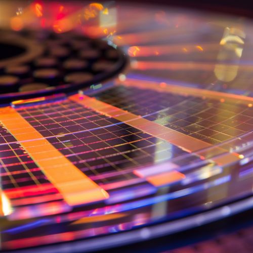
Lithography and etching processes are used to define the laser's structure and create the necessary patterns on the semiconductor wafer. Photolithography involves using light to transfer a pattern onto a photosensitive material, while etching removes unwanted material to create the desired features.
Applications of Quantum Well Lasers
Quantum well lasers have a wide range of applications due to their superior performance characteristics, including high efficiency, low threshold current, and wavelength tunability.
Telecommunications
In telecommunications, quantum well lasers are used in fiber optic communication systems to transmit data over long distances with minimal loss. Their ability to operate at specific wavelengths, such as 1.3 µm and 1.55 µm, makes them ideal for use in optical fibers with low attenuation.
Medical Devices
Quantum well lasers are employed in various medical devices, including surgical instruments, diagnostic equipment, and therapeutic devices. Their precise wavelength control and high power output make them suitable for applications such as laser surgery, photodynamic therapy, and optical coherence tomography.
Optical Data Storage
In optical data storage, quantum well lasers are used in devices such as CD, DVD, and Blu-ray players. The lasers' ability to emit light at specific wavelengths allows for the reading and writing of data on optical discs with high precision and density.
Advantages and Challenges
Quantum well lasers offer several advantages over conventional semiconductor lasers, but they also present certain challenges.
Advantages
- **High Efficiency:** Quantum well lasers have higher efficiency due to enhanced carrier confinement and increased radiative recombination rates.
- **Low Threshold Current:** The threshold current, the minimum current required to achieve lasing, is lower in quantum well lasers, leading to reduced power consumption.
- **Wavelength Tunability:** The ability to tailor the bandgap allows for precise control over the emission wavelength, making quantum well lasers versatile for various applications.
Challenges
- **Fabrication Complexity:** The fabrication of quantum well lasers requires advanced techniques and precise control over layer thickness and composition, making the process complex and costly.
- **Thermal Management:** Managing the heat generated during operation is crucial to maintain the performance and reliability of quantum well lasers.
- **Material Quality:** High-quality materials with minimal defects are essential to achieve the desired performance, necessitating stringent quality control during fabrication.
Future Developments
The field of quantum well lasers continues to evolve, with ongoing research and development aimed at improving performance and expanding applications.
Quantum Dot Lasers
Quantum dot lasers, which utilize quantum dots instead of quantum wells, are an emerging technology with the potential to offer even greater efficiency and performance. Quantum dots provide three-dimensional confinement, leading to further enhancement of optical properties.
Integration with Photonic Circuits
The integration of quantum well lasers with photonic circuits is a promising area of research. This integration aims to create compact, high-performance optical systems for applications in telecommunications, computing, and sensing.
Advanced Materials
The development of new materials with superior properties, such as higher thermal conductivity and better lattice matching, is crucial for advancing quantum well laser technology. Research in materials science is focused on discovering and optimizing such materials.
See Also
- Semiconductor Laser
- Quantum Dot Laser
- Optical Fiber Communication
- Photonic Integrated Circuit
- Molecular Beam Epitaxy
- Metal-Organic Chemical Vapor Deposition
