Molecular Beam Epitaxy
Introduction
Molecular Beam Epitaxy (MBE) is a method of depositing single crystals. It was developed in the late 1960s at Bell Telephone Laboratories as a technique to fabricate single-crystal semiconductor layers for manufacturing transistors and diodes. The technique is widely used in the manufacture of semiconductor devices, including transistors, diodes, and integrated circuits.
History
The concept of MBE was first introduced by J.R. Arthur and Alfred Y. Cho at Bell Labs in 1968. Their work was initially focused on the growth of gallium arsenide (GaAs) and aluminum gallium arsenide (AlGaAs) layers on GaAs substrates. The technique was later extended to other materials, including indium phosphide (InP), gallium nitride (GaN), and silicon (Si).
Principle of Operation
MBE is a type of physical vapor deposition (PVD) technique. It operates under ultra-high vacuum (UHV) conditions, typically at pressures of 10^-10 torr or lower. The process involves heating a solid source material to produce a beam of atoms or molecules, which is then directed towards a heated substrate. The atoms or molecules in the beam arrive at the substrate with a low kinetic energy, allowing them to migrate on the surface and nucleate into a crystal structure that matches the lattice of the substrate.
Equipment
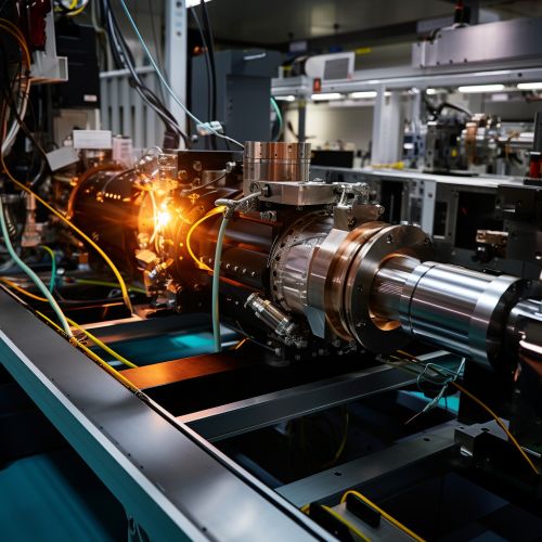
An MBE system typically consists of an ultra-high vacuum chamber, source material holders (known as "effusion cells" or "Knudsen cells"), a substrate holder (or "wafer platen"), and a system for monitoring and controlling the growth process. The effusion cells are heated to evaporate the source material, and the wafer platen is heated to a temperature suitable for crystal growth. The growth process is monitored and controlled using techniques such as reflection high-energy electron diffraction (RHEED) and quartz crystal microbalance (QCM).


Growth Process
The growth process in MBE involves several steps. First, the substrate is prepared by cleaning and heating to remove any surface contamination. The source materials are then heated to produce atomic or molecular beams, which are directed towards the substrate. The atoms or molecules in the beams arrive at the substrate with a low kinetic energy, allowing them to migrate on the surface and nucleate into a crystal structure that matches the lattice of the substrate. The growth rate is typically on the order of one monolayer per second.
Applications
MBE is used in the fabrication of a wide range of semiconductor devices, including transistors, diodes, and integrated circuits. It is also used in the growth of thin films for optoelectronic devices, such as light-emitting diodes (LEDs) and laser diodes. In addition, MBE is used in the growth of superlattices, quantum wells, and other nanostructured materials.
Advantages and Disadvantages
MBE has several advantages over other thin film deposition techniques. It allows for precise control over the thickness and composition of the deposited layers, and it can produce high-quality single-crystal films. However, MBE also has some disadvantages. It is a slow process, and it requires a high level of vacuum, which can be difficult and expensive to maintain. In addition, the source materials used in MBE are often toxic and require careful handling.
