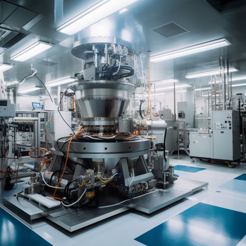
Electron Beam Lithography
Introduction
Electron Beam Lithography (EBL) is a method of etching semiconductors at a very high resolution, using a focused beam of electrons. This technique is primarily used in the semiconductor industry for the fabrication of integrated circuits (ICs) and other microdevices.


History
The concept of Electron Beam Lithography was first introduced in the 1960s, as a result of advancements in electron microscopy. The first commercial EBL systems were developed in the 1970s, and since then, the technology has evolved significantly, becoming a vital tool in the semiconductor industry.
Working Principle
The working principle of EBL involves the use of a focused beam of electrons to create patterns on a substrate coated with an electron-sensitive film called a resist. The electron beam changes the solubility of the resist, enabling selective removal of either exposed or non-exposed regions of the resist by an appropriate developer solution.
Components of an EBL System
An EBL system comprises several key components, including an electron gun, a beam blanker, a lens system, a stage, and a computer control system.
Electron Gun
The electron gun generates and accelerates the electrons. The quality of the electron beam, which is crucial for the resolution of the lithography, is determined by the design of the electron gun.
Beam Blanker
The beam blanker is used to control the exposure of the electron beam. It can rapidly switch the electron beam on and off, allowing for precise control over the exposure of the resist.
Lens System
The lens system focuses the electron beam onto the resist-coated substrate. The resolution of the lithography is highly dependent on the quality of the lens system.
Stage
The stage holds the substrate and can move in x, y, and z directions. The movement of the stage is controlled by the computer system, allowing for precise positioning of the substrate.
Computer Control System
The computer control system coordinates the operation of the other components. It controls the beam blanker, the lens system, and the stage, and also processes the data required for the lithography.
Applications
EBL is used in a variety of applications, primarily in the semiconductor industry. It is used for the fabrication of integrated circuits, micro-electro-mechanical systems (MEMS), and nanodevices. It is also used in research and development, particularly in the field of nanotechnology.
Advantages and Limitations
EBL offers several advantages, including high resolution, flexibility in pattern design, and the ability to create complex structures. However, it also has some limitations, such as slow throughput, high cost, and the requirement for a cleanroom environment.
Future Trends
The future of EBL is likely to be influenced by advancements in electron beam technology, improvements in resist materials, and the increasing demand for miniaturization in the semiconductor industry.
