Deep reactive-ion etching
Introduction
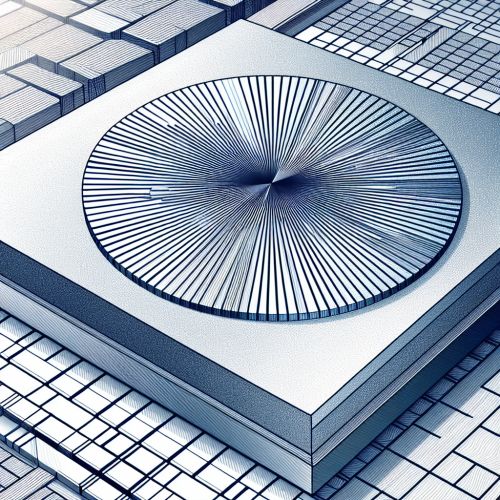
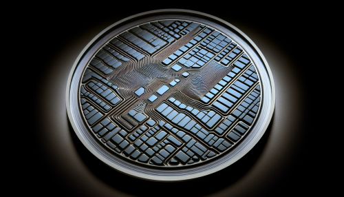
Deep reactive-ion etching (DRIE) is a highly anisotropic etch process used to create deep penetration, steep-sided holes and trenches in wafers/substrates, typically with high aspect ratios. It was developed for microelectromechanical systems (MEMS), which require these features, but is also used to excavate trenches for high-density capacitors for DRAM production.
History
The development of DRIE technology was driven by the need for high aspect ratio structures in MEMS. The first DRIE processes were developed in the mid-1990s, with the key breakthrough being the Bosch process, named after the Robert Bosch company, which patented the process. The Bosch process allowed for the creation of high aspect ratio structures with nearly vertical sidewalls, which was a significant improvement over previous etching techniques.
Process
DRIE is achieved by alternately etching and passivating the substrate. The etching is performed by a plasma of reactive ions, such as sulfur hexafluoride (SF6). The passivation, or protection, of the etched surface is performed using a plasma polymerizing agent, such as octafluorocyclobutane (C4F8). This process results in a series of scallops or ripples on the sidewalls of the etched structures.
Bosch Process
The Bosch process is the most commonly used method for DRIE. It is a two-step process, alternating between etching and passivation. The etching step uses SF6, which is a strong etchant that reacts with silicon to form silicon tetrafluoride (SiF4), a volatile gas. The passivation step uses C4F8, which forms a protective polymer on the surface of the silicon. This polymer is resistant to the SF6 etch, but is sputtered away by the physical ion bombardment, allowing the etch to proceed.
Cryogenic Process
An alternative to the Bosch process is the cryogenic process, which uses very low temperatures to slow the chemical reaction rate and increase the physical sputtering rate. This results in a smoother etch profile and smaller scallops than the Bosch process, but at the cost of a slower etch rate and higher energy consumption.
Applications
DRIE is used in a variety of applications, including MEMS, nanotechnology, and semiconductor manufacturing. In MEMS, it is used to create high aspect ratio structures, such as accelerometers and gyroscopes. In nanotechnology, it is used to create nanopillars and nanowires. In semiconductor manufacturing, it is used to create deep trenches for DRAM and 3D NAND flash memory.
Advantages and Disadvantages
The main advantage of DRIE is its ability to create high aspect ratio structures with nearly vertical sidewalls. This is essential for many MEMS and semiconductor applications. However, DRIE also has some disadvantages. The process is complex and requires precise control of many parameters. The etched structures also have scalloped sidewalls, which can be a problem for some applications.
See Also


