X-ray lithography
Introduction
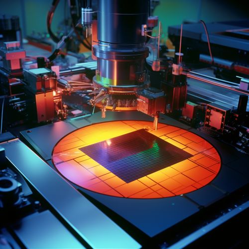
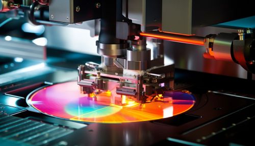
X-ray lithography, also known as XRL, is a process used in electronic industry to accurately print tiny geometric shapes on silicon wafers (or any other substrates) which are then used in the manufacturing of integrated circuits (ICs) and microelectromechanical systems (MEMS). This technique utilizes X-rays to transfer a geometric pattern from a mask to a light-sensitive chemical photoresist, or simply "resist," on the substrate. X-ray lithography is part of a broader category of photolithographic techniques, which also includes ultraviolet (UV) and extreme ultraviolet (EUV) lithography.


History
The concept of X-ray lithography was first introduced in the late 1970s, as a response to the limitations of traditional optical lithography. As the demand for smaller and more efficient ICs grew, the need for a more precise lithographic technique became apparent. The use of X-rays, with their shorter wavelength, provided a solution to this problem, allowing for the creation of smaller and more precise geometric patterns.
Process
The process of X-ray lithography begins with the preparation of the substrate, usually a silicon wafer, which is cleaned and coated with a layer of photoresist. The photoresist is a light-sensitive material that changes its properties when exposed to light (in this case, X-rays). The wafer is then placed under a mask, which contains the desired geometric pattern. The mask and the wafer are then exposed to X-rays. The X-rays pass through the clear areas of the mask and are absorbed by the photoresist on the wafer, causing it to undergo a chemical change. After exposure, the wafer is developed, removing the areas of photoresist that were exposed to the X-rays and leaving behind the desired pattern.
Advantages and Disadvantages
One of the main advantages of X-ray lithography is its ability to create very small and precise geometric patterns, down to a few nanometers in size. This makes it ideal for the production of ICs and MEMS, where precision and miniaturization are key. Furthermore, because X-rays are not easily deflected or scattered, X-ray lithography can produce patterns with very straight sidewalls, which is important in many applications.
However, X-ray lithography also has its disadvantages. The process requires a high degree of precision and control, and is therefore more complex and expensive than other lithographic techniques. Additionally, the use of X-rays presents safety concerns, as they are a form of ionizing radiation.
Applications
X-ray lithography is primarily used in the production of ICs and MEMS. In IC production, it is used to create the intricate patterns of transistors and other components on a silicon wafer. In MEMS production, it is used to create the tiny mechanical components that make up these systems.
Future Developments
As the demand for smaller and more efficient electronic devices continues to grow, the importance of X-ray lithography is likely to increase. Researchers are continually working on ways to improve the process, making it more efficient and cost-effective. One area of focus is the development of new photoresists that are more sensitive to X-rays, which could reduce the amount of exposure time required and therefore increase throughput.
