Scanning Tunneling Microscopy
Introduction
Scanning tunneling microscopy (STM) is a powerful technique for viewing surfaces at the atomic level. The method exploits the quantum mechanical phenomenon known as tunneling, in which particles can pass through potential barriers that would be insurmountable in classical physics.


Principle of Operation
The STM operates by bringing a sharp metal tip in close proximity to a surface. A bias voltage is applied between the tip and the surface, causing electrons to tunnel across the vacuum gap between the two. The tunneling current, which is highly sensitive to the distance between the tip and the surface, is measured as the tip scans across the surface. This current is then used to generate an image of the surface topography at the atomic scale.
History
The scanning tunneling microscope was invented in 1981 by Gerd Binnig and Heinrich Rohrer at the IBM Zurich Research Lab. Their pioneering work on STM earned them the Nobel Prize in Physics in 1986.
Instrumentation
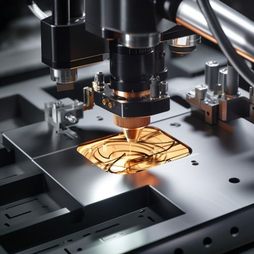
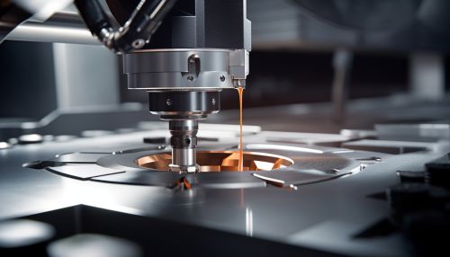
The key components of an STM include the scanning tip, piezoelectric scanner, sample holder, vibration isolation system, and the electronic control and data acquisition system. The scanning tip is usually made of tungsten or platinum-iridium, and is prepared to be atomically sharp. The piezoelectric scanner moves the tip in three dimensions with respect to the sample, allowing the tip to scan the surface.
Applications
Scanning tunneling microscopy has found wide application in various fields such as physics, chemistry, materials science, and biology. It has been used to study a variety of surfaces ranging from metals, semiconductors, superconductors, and topological insulators to thin films, single molecules, and even biological samples.
Limitations and Challenges
While STM provides unparalleled spatial resolution, it also has certain limitations. The method requires conductive samples, and is not suitable for insulating materials. The technique is also surface-sensitive, and cannot provide information about the bulk properties of a material. Furthermore, the interpretation of STM images requires careful consideration of the electronic structure of the sample and the tip.
Future Directions
Future developments in STM technology may include the integration of other techniques such as atomic force microscopy (AFM) and spectroscopy to provide complementary information about the sample. The development of new tip materials and imaging modes may also expand the range of samples that can be studied with STM.
