Scanning Tunneling Microscope
Introduction
The Scanning Tunneling Microscope (STM) is a type of electron microscope that provides three-dimensional profiling of surfaces at the atomic level. The STM is a non-optical microscope that uses the principles of quantum mechanics to create images of surfaces. It was invented in 1981 by Gerd Binnig and Heinrich Rohrer at IBM Zurich Research Laboratory, for which they received the Nobel Prize in Physics in 1986.
Principle of Operation
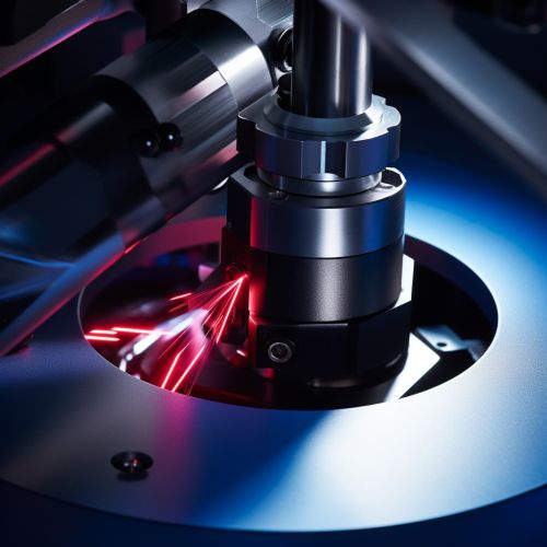
The STM operates based on the concept of Quantum Tunneling. When a conducting tip is brought very near to the surface to be examined, a bias (voltage difference) applied between the two can allow electrons to tunnel through the vacuum between them. The resulting tunneling current is a function of tip position, applied voltage, and the local density of states (LDOS) of the sample. Information is acquired by monitoring the current as the tip's position scans across the surface, and is usually displayed in image form.


Components
The key components of an STM include the scanning tip, piezoelectric controlled height and x,y scanner, coarse sample-to-tip control, vibration isolation system, and computer system for data acquisition. The resolution of an image is limited by the radius of curvature of the scanning tip of the STM. Additionally, image artifacts can occur if the tip has two tips at the end rather than a single atom; this leads to “double-tip imaging,” a situation in which both tips contribute to the tunneling.
Applications
The STM can be used not only in ultra-high vacuum but also in air, water, and various other liquid and gas ambients and at temperatures ranging from near zero kelvin to a few hundred degrees Celsius. The STM is considered a prime example of nanotechnology. It was the first device that enabled scientists to visualize the world on the atomic scale, and it can be used to manipulate atoms and molecules to create or modify structures at the atomic level.
Advantages and Limitations
The STM has several advantages over other microscopy techniques. It can produce images of high resolution of the surfaces of metals and semiconductors, it requires relatively minimal sample preparation, and it can be used to image both conducting and non-conducting surfaces. On the other hand, the types of samples that can be imaged are limited because the STM requires a conductive sample surface. Furthermore, the STM cannot provide chemical information about the atoms on the surface.
