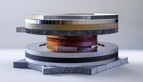
Quantum wells
Introduction
A quantum well is a potential well that confines particles, which are often electrons or holes, to motion in one dimension, forcing them to occupy discrete energy levels. Quantum wells are a foundational concept in quantum mechanics and semiconductor physics, playing a crucial role in the development of modern electronic and optoelectronic devices.
Theory and Principles
Quantum wells are typically formed by sandwiching a thin layer of a semiconductor material with a smaller bandgap between two layers of a semiconductor with a larger bandgap. This creates a potential energy profile that confines charge carriers in the thin layer, leading to quantization of their energy levels.
Schrödinger Equation in Quantum Wells
The behavior of particles in a quantum well can be described by the Schrödinger equation. For a particle of mass \( m \) in a one-dimensional potential well of width \( L \), the time-independent Schrödinger equation is given by: \[ -\frac{\hbar^2}{2m} \frac{d^2 \psi(x)}{dx^2} + V(x) \psi(x) = E \psi(x) \] where \( \hbar \) is the reduced Planck constant, \( \psi(x) \) is the wavefunction, \( V(x) \) is the potential energy, and \( E \) is the energy of the particle.
Energy Levels and Wavefunctions
In an idealized infinite potential well, the energy levels are given by: \[ E_n = \frac{n^2 \pi^2 \hbar^2}{2mL^2} \] where \( n \) is a positive integer representing the quantum number. The corresponding wavefunctions are: \[ \psi_n(x) = \sqrt{\frac{2}{L}} \sin\left(\frac{n \pi x}{L}\right) \]
In a more realistic finite potential well, the energy levels and wavefunctions are determined by solving the Schrödinger equation with appropriate boundary conditions, leading to a more complex set of solutions.
Fabrication Techniques
Quantum wells are typically fabricated using advanced semiconductor growth techniques such as molecular beam epitaxy (MBE) and metal-organic chemical vapor deposition (MOCVD). These methods allow for precise control over the thickness and composition of the layers, which is crucial for achieving the desired quantum confinement effects.
Molecular Beam Epitaxy (MBE)
MBE is a highly controlled process where atomic or molecular beams of the constituent materials are directed onto a heated substrate in an ultra-high vacuum environment. This technique allows for the growth of high-quality, atomically precise layers, making it ideal for creating quantum wells.
Metal-Organic Chemical Vapor Deposition (MOCVD)
MOCVD involves the chemical reaction of metal-organic compounds with other gases to deposit thin films on a substrate. This method is widely used in the semiconductor industry for its ability to produce large-area, uniform layers with good control over composition and thickness.
Applications
Quantum wells have a wide range of applications in modern technology, particularly in the fields of electronics and optoelectronics.
Lasers and Light-Emitting Diodes (LEDs)
Quantum wells are used in the active regions of semiconductor lasers and LEDs to enhance performance by providing higher carrier confinement and increased recombination rates. This leads to devices with higher efficiency and lower threshold currents.
High-Electron-Mobility Transistors (HEMTs)
HEMTs utilize quantum wells to create a two-dimensional electron gas (2DEG) with high electron mobility, resulting in transistors with superior performance characteristics such as higher speed and lower noise.
Quantum Cascade Lasers
Quantum cascade lasers (QCLs) exploit the intersubband transitions in quantum wells to produce coherent light in the mid-infrared to terahertz range. QCLs are used in applications such as gas sensing, spectroscopy, and free-space communication.
Advanced Concepts
Quantum wells serve as a platform for exploring more advanced concepts in quantum mechanics and semiconductor physics.
Quantum Well Intermixing (QWI)
QWI is a technique used to modify the bandgap of quantum wells post-growth by inducing interdiffusion of atoms across the well and barrier layers. This allows for the tuning of optical and electronic properties, enabling the fabrication of complex integrated photonic devices.
Quantum Confined Stark Effect (QCSE)
The QCSE refers to the shift in the energy levels of a quantum well under the influence of an external electric field. This effect is utilized in electro-absorption modulators and other optoelectronic devices to control light propagation through the material.
Excitonic Effects
In quantum wells, the confinement of electrons and holes leads to the formation of excitons, which are bound states of an electron and a hole. Excitonic effects play a significant role in the optical properties of quantum wells, influencing absorption and emission spectra.
Experimental Techniques
Several experimental techniques are used to study and characterize quantum wells.
Photoluminescence Spectroscopy
Photoluminescence spectroscopy involves exciting the quantum well with a light source and measuring the emitted light. This technique provides information about the energy levels, recombination processes, and material quality.
Absorption Spectroscopy
Absorption spectroscopy measures the absorption of light as a function of wavelength, revealing details about the electronic transitions and band structure of the quantum well.
Scanning Tunneling Microscopy (STM)
STM is a powerful tool for imaging the surface of quantum wells at the atomic scale. It provides insights into the structural and electronic properties of the material.
Challenges and Future Directions
While quantum wells have enabled significant advancements in technology, several challenges and opportunities for future research remain.
Material Quality and Interface Roughness
The performance of quantum well devices is highly dependent on the quality of the materials and the smoothness of the interfaces. Advances in growth techniques and materials science are needed to further improve these aspects.
Quantum Well Infrared Photodetectors (QWIPs)
QWIPs are devices that utilize intersubband transitions in quantum wells to detect infrared light. Research is ongoing to enhance their sensitivity and operating wavelength range.
Integration with Other Quantum Structures
Combining quantum wells with other quantum structures such as quantum dots and quantum wires offers the potential for new device functionalities and enhanced performance. This area of research is expected to yield exciting developments in the coming years.


See Also
- Quantum Mechanics
- Semiconductor Physics
- Molecular Beam Epitaxy
- High-Electron-Mobility Transistor
- Quantum Cascade Laser
