Microcontact Printing
Introduction
Microcontact printing (μCP) is a form of soft lithography that uses a patterned stamp to deposit a material onto a substrate. This technique is widely used in the fields of nanotechnology, materials science, and bioengineering due to its ability to create precise, microscale patterns on a variety of surfaces.


Process
The process of microcontact printing begins with the creation of a master mold, typically made from silicon or a similar material. The mold is patterned using photolithography or another suitable technique, and then a liquid pre-polymer, such as polydimethylsiloxane (PDMS), is poured over the mold and cured. Once cured, the PDMS stamp is peeled off, revealing a patterned surface that can be used to print onto a substrate.
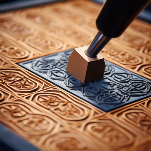
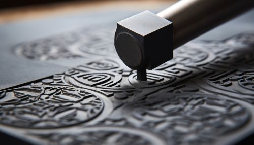
The stamp is then inked with the desired material, which can range from organic molecules to nanoparticles. The inked stamp is brought into contact with the substrate, transferring the patterned material. The process can be repeated multiple times on the same substrate, allowing for the creation of complex, multi-layered structures.
Applications
Microcontact printing has a wide range of applications due to its versatility and precision. In the field of nanotechnology, it is used to create nanostructures and nanodevices. In materials science, it is used to pattern surfaces for studies of material properties. In bioengineering, it is used to pattern biomolecules on surfaces for cell culture studies.
Nanotechnology
In nanotechnology, microcontact printing is used to create structures at the nanoscale. This is particularly useful for the fabrication of nanodevices, such as nanowires, nanotubes, and quantum dots. The ability to precisely control the placement and arrangement of these structures is crucial for their functionality.
Materials Science
In materials science, microcontact printing is used to create patterned surfaces for studying material properties. For example, it can be used to pattern a thin film of a material onto a substrate, allowing for the study of the film's electrical or optical properties. It can also be used to create patterned adhesive surfaces for studying the adhesion properties of different materials.
Bioengineering
In bioengineering, microcontact printing is used to pattern biomolecules on surfaces for cell culture studies. This is particularly useful for studying cell behavior in response to different environmental cues. For example, it can be used to pattern proteins on a surface to study cell adhesion, migration, and differentiation.
Advantages and Limitations
Microcontact printing offers several advantages over other patterning techniques. It is a relatively simple and inexpensive process, requiring only a patterned stamp and a substrate. It is also a versatile technique, capable of patterning a wide range of materials onto various substrates. Furthermore, it can create patterns with high resolution and precision, making it suitable for creating complex, microscale structures.
However, microcontact printing also has some limitations. The quality of the printed pattern can be affected by several factors, including the properties of the stamp and the ink, the contact pressure and time, and the surface properties of the substrate. Additionally, while it can create high-resolution patterns, it is not as precise as some other techniques, such as electron-beam lithography.
Future Directions
The field of microcontact printing continues to evolve, with ongoing research aimed at improving the technique and expanding its applications. One area of focus is the development of new materials for the stamp and the ink, which could improve the quality of the printed patterns and expand the range of materials that can be patterned. Another area of focus is the integration of microcontact printing with other techniques, such as nanofabrication, to create more complex structures.
