Diode Sputtering
Introduction
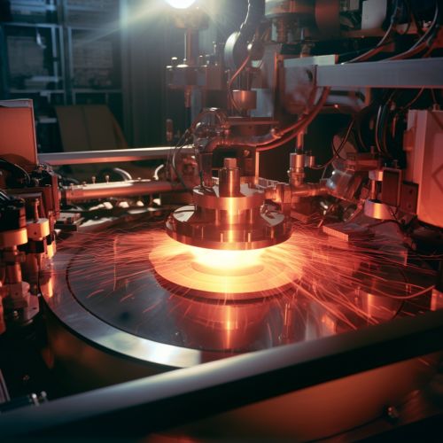
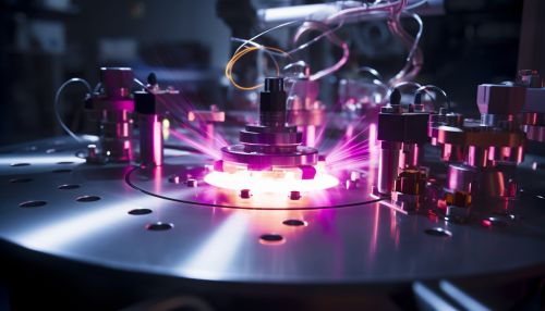
Diode sputtering is a physical vapor deposition (PVD) process used in the fabrication of thin films. The process involves the use of a diode, which is a two-terminal electronic component that conducts current primarily in one direction. In the context of sputtering, a diode is used to create a plasma environment that facilitates the ejection of atoms from a target material, which then deposit onto a substrate to form a thin film.
Principles of Diode Sputtering
Diode sputtering operates on the principles of plasma physics and surface science. A plasma is generated by applying a high voltage between the cathode (target material) and the anode (usually the chamber wall or substrate holder). The electric field accelerates ions in the plasma towards the cathode, causing atoms to be ejected from the target due to momentum transfer. These ejected atoms then travel across the plasma and deposit onto the substrate, forming a thin film.


Diode Sputtering Systems
Diode sputtering systems typically consist of a vacuum chamber, a gas supply, a power supply, a target holder (cathode), and a substrate holder (anode). The vacuum chamber is necessary to maintain a low-pressure environment, which allows the sputtering process to occur. The gas supply provides the working gas, usually an inert gas such as argon, which is ionized to form the plasma. The power supply provides the high voltage necessary to generate the plasma and accelerate the ions towards the target.
Process Parameters
Several parameters influence the diode sputtering process and the properties of the resulting thin films. These include the sputtering gas pressure, the applied voltage, the target-to-substrate distance, and the type of target material. Adjusting these parameters allows control over the deposition rate, film thickness, and film properties such as density, stress, and crystallographic orientation.
Applications
Diode sputtering is widely used in various industries for the fabrication of thin films. In the semiconductor industry, it is used for the deposition of metal and dielectric layers in integrated circuits. In the optics industry, it is used to produce optical coatings for lenses and mirrors. It is also used in the fabrication of solar cells, data storage devices, and surface coating applications.
Advantages and Limitations
Diode sputtering offers several advantages, including high deposition rates, good film uniformity, and the ability to coat large areas. It is also a relatively simple and cost-effective process. However, it also has some limitations. For example, it requires line-of-sight between the target and substrate, which can make it difficult to coat complex geometries. It also tends to produce films with high intrinsic stress, which can lead to film cracking or delamination.
