Czochralski process
Introduction
The Czochralski process is a method of crystal growth used to obtain single crystals of semiconductors (e.g., silicon, germanium and gallium arsenide), metals (e.g., palladium, platinum, silver, gold), salts and synthetic gemstones. The process is named after Polish scientist Jan Czochralski, who invented the method in 1915 while investigating the crystallization rates of metals.
History
The Czochralski process was discovered somewhat accidentally by Jan Czochralski, a Polish scientist working in Germany. In 1915, while studying the crystallization rates of metals, he accidentally dipped his pen into a crucible of molten tin rather than his inkwell. He immediately pulled his pen out to find a thin thread of solidified metal hanging from the nib. This observation led him to develop the Czochralski process.


Process Description
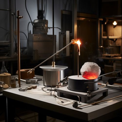
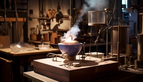
The Czochralski process begins by melting a large quantity of the material in a crucible. A small seed crystal mounted on a rod is dipped into the molten phase. The rod is then slowly pulled upwards and rotated simultaneously. By precisely controlling the temperature gradients, rate of pulling and speed of rotation, it is possible to extract a large, single-crystal, cylindrical ingot from the melt.
Crucible
The crucible material must be carefully chosen for its non-reactivity with the molten phase. For instance, when growing silicon crystals, high-purity quartz is typically used.
Seed Crystal
The seed crystal's characteristics are critical in determining the final crystal's properties, such as orientation, size, and the presence of any defects. The seed crystal is often prepared by a separate process, such as the Bridgman–Stockbarger technique, before being used in the Czochralski process.
Temperature Control
Precise control of temperature is crucial in the Czochralski process. The temperature of the melt, the temperature gradient in the melt, and the temperature of the growing crystal must all be carefully controlled to ensure the growth of a single crystal.
Applications
The Czochralski process is widely used in the production of semiconductor crystals for use in electronics, particularly in the manufacture of computer chips. Silicon wafers, the most common semiconductor, are almost all manufactured using the Czochralski process. Other materials, such as gallium arsenide, are also grown using this method. In addition, the process is used to produce synthetic gemstones, and large, high-quality crystals of rare earth metals for use in lasers.
Advantages and Disadvantages
The main advantage of the Czochralski process is that it can produce large, high-quality single crystals with few defects. However, the process is not without its disadvantages. It is a slow and energy-intensive process, and it requires a large amount of starting material, much of which is wasted during the crystal growth process.
