VLSI Design
Introduction
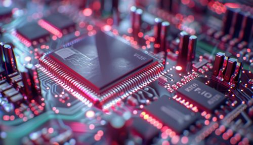
Very Large Scale Integration (VLSI) Design refers to the process of creating an integrated circuit (IC) by combining thousands of transistors into a single chip. VLSI technology was conceived in the late 1970s when advanced level computer processor microchips were under development. VLSI lets IC designers add all of the components of an electronic circuit into one single chip.


History and Evolution
The concept of VLSI design was first introduced by Carver Mead and Lynn Conway in their seminal work "Introduction to VLSI Systems". The advent of VLSI technology marked a significant turning point in the semiconductor industry, enabling the design and fabrication of complex ICs.
The evolution of VLSI technology can be categorized into different generations, each characterized by the minimum feature size of the components. The first generation of VLSI devices had minimum feature sizes of 10 micrometers. This was followed by the second generation, with feature sizes of 3 micrometers, and the third generation, with feature sizes of 1 micrometer.
VLSI Design Process
The VLSI design process involves several stages, each with its own set of tasks and objectives. These stages include system specification, architectural design, functional design, logic design, circuit design, physical design, and verification.
System Specification
The system specification stage involves defining the functionality, performance, physical constraints, and other high-level requirements of the IC. This stage is crucial for setting the direction of the entire design process.
Architectural Design
In the architectural design stage, the system specifications are translated into a detailed system architecture. This involves defining the data path, control unit, memory organization, and other architectural elements of the IC.
Functional Design
The functional design stage involves the development of a detailed functional description of the IC. This is typically done using a hardware description language (HDL) such as VHDL or Verilog.
Logic Design
The logic design stage involves converting the functional description into a logic representation. This involves the use of logic gates and flip-flops to implement the desired functionality.
Circuit Design
In the circuit design stage, the logic representation is converted into a circuit representation. This involves the selection of specific circuit technologies and the design of individual circuit elements.
Physical Design
The physical design stage involves the layout of the IC, including the placement of circuit elements and the routing of interconnections. This stage is crucial for ensuring that the IC meets its performance and physical constraints.
Verification
The verification stage involves checking that the IC meets its specified functionality and performance. This is typically done through simulation and testing.
VLSI Design Techniques
There are several techniques used in VLSI design, including full custom design, semi-custom design, and programmable logic design.
Full Custom Design
Full custom design involves the design of the entire IC from scratch. This approach allows for maximum performance and minimum size, but it is also the most time-consuming and expensive.
Semi-Custom Design
Semi-custom design involves the use of pre-designed circuit blocks, or cells, which are then customized to meet the specific requirements of the IC. This approach offers a balance between performance, size, and design time.
Programmable Logic Design
Programmable logic design involves the use of programmable logic devices (PLDs), which can be configured to implement a wide range of digital circuits. This approach offers the fastest design time, but it also has the lowest performance and the largest size.
VLSI Design Tools
There are several types of tools used in VLSI design, including synthesis tools, simulation tools, and physical design tools.
Synthesis Tools
Synthesis tools are used to convert a high-level description of the IC into a lower-level representation. This includes logic synthesis tools, which convert a functional description into a logic representation, and physical synthesis tools, which convert a logic representation into a physical layout.
Simulation Tools
Simulation tools are used to verify the functionality and performance of the IC. This includes functional simulation tools, which check the correctness of the IC's functionality, and timing simulation tools, which check the IC's performance.
Physical Design Tools
Physical design tools are used to create the physical layout of the IC. This includes placement tools, which determine the locations of the circuit elements, and routing tools, which determine the paths of the interconnections.
Future Trends in VLSI Design
The future of VLSI design is likely to be characterized by continued miniaturization, increased complexity, and new materials and technologies. One of the key trends is the move towards nanoscale devices, with feature sizes of less than 100 nanometers. This will require new design techniques and tools, as well as new fabrication processes.
Another key trend is the increasing complexity of ICs, with the integration of billions of transistors on a single chip. This will require advanced design methodologies and tools, as well as new ways of managing the complexity.
Finally, new materials and technologies are likely to play a key role in the future of VLSI design. This includes the use of new semiconductor materials, such as silicon germanium and gallium arsenide, as well as new device technologies, such as quantum devices and spintronics.
