Low Pressure Chemical Vapor Deposition
Introduction
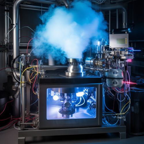
Low Pressure Chemical Vapor Deposition (LPCVD) is a process used in semiconductor manufacturing to deposit thin films from a gas state (vapor) onto a substrate. In LPCVD systems, the wafer (substrate) is exposed to one or more volatile precursors, which react and/or decompose on the substrate surface to produce the desired deposit. The process operates at a lower pressure to enhance chemical reactions and improve film uniformity.
Process Overview
The LPCVD process begins with the placement of a semiconductor wafer into a deposition chamber. The chamber is then evacuated to a low pressure, typically in the range of 0.1 to 2 Torr. The wafer is then heated to a high temperature, often between 450 and 850 degrees Celsius, depending on the specific process. Once the appropriate temperature and pressure are reached, the volatile precursors are introduced into the chamber. These precursors react with the wafer surface, depositing a thin film of material. The byproducts of this reaction are then removed from the chamber by the vacuum system.


Advantages of LPCVD
LPCVD offers several advantages over other deposition methods. First, it allows for the deposition of films with excellent uniformity over large areas. This is particularly important in semiconductor manufacturing, where wafers can be up to 300mm in diameter. Second, LPCVD processes can be highly automated, allowing for high throughput and low cost. Finally, because the process operates at low pressure, it is less susceptible to contamination from the surrounding environment, leading to higher quality films.
Applications of LPCVD
LPCVD is used in a variety of applications in semiconductor manufacturing. These include the deposition of silicon nitride and silicon dioxide for gate dielectrics, the deposition of polysilicon for gate electrodes, and the deposition of metal-organic chemical vapor deposition (MOCVD) for compound semiconductor devices. In addition to these applications, LPCVD is also used to deposit films for microelectromechanical systems (MEMS), solar cells, and other thin film applications.
Challenges and Limitations
While LPCVD offers many advantages, it also has some limitations. The process requires high temperatures, which can be a challenge for certain applications. Additionally, the precursors used in LPCVD are often hazardous, requiring careful handling and disposal. Finally, while LPCVD allows for excellent film uniformity, it can be difficult to control the composition of the film, particularly for complex materials.
Future Developments
As the demand for smaller and more complex devices continues to grow, the role of LPCVD in semiconductor manufacturing is likely to expand. Researchers are currently exploring new materials and processes that can be used with LPCVD, as well as ways to improve the efficiency and safety of the process. In particular, there is significant interest in developing LPCVD processes for the deposition of high-k dielectrics and advanced barrier materials.
