Phototransistor: Difference between revisions
(Created page with "== Introduction == A '''phototransistor''' is a type of transistor that operates as a photodetector. It is a semiconductor device that converts light into an electrical signal. Phototransistors are widely used in various applications, including optical communication, light sensing, and automatic lighting control systems. They offer higher sensitivity compared to photodiodes due to their internal gain mechanism. == Structure and Operation == Pho...") |
No edit summary |
||
| Line 7: | Line 7: | ||
Phototransistors are typically made from [[silicon]] or [[gallium arsenide]]. The basic structure of a phototransistor includes a [[base]], [[collector]], and [[emitter]], similar to a [[bipolar junction transistor]] (BJT). However, in a phototransistor, the base region is exposed to light, and the incident photons generate electron-hole pairs. These charge carriers are then amplified by the transistor's gain mechanism, resulting in a significant increase in the collector current. | Phototransistors are typically made from [[silicon]] or [[gallium arsenide]]. The basic structure of a phototransistor includes a [[base]], [[collector]], and [[emitter]], similar to a [[bipolar junction transistor]] (BJT). However, in a phototransistor, the base region is exposed to light, and the incident photons generate electron-hole pairs. These charge carriers are then amplified by the transistor's gain mechanism, resulting in a significant increase in the collector current. | ||
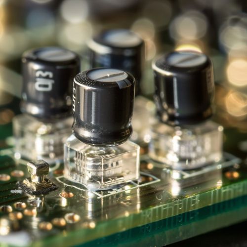
[[Image:Detail-79199.jpg|thumb|center|Close-up image of a phototransistor with visible base, collector, and emitter terminals.|class=only_on_mobile]] | |||
[[Image:Detail-79200.jpg|thumb|center|Close-up image of a phototransistor with visible base, collector, and emitter terminals.|class=only_on_desktop]] | |||
== Types of Phototransistors == | == Types of Phototransistors == | ||
Latest revision as of 13:24, 17 May 2024
Introduction
A phototransistor is a type of transistor that operates as a photodetector. It is a semiconductor device that converts light into an electrical signal. Phototransistors are widely used in various applications, including optical communication, light sensing, and automatic lighting control systems. They offer higher sensitivity compared to photodiodes due to their internal gain mechanism.
Structure and Operation
Phototransistors are typically made from silicon or gallium arsenide. The basic structure of a phototransistor includes a base, collector, and emitter, similar to a bipolar junction transistor (BJT). However, in a phototransistor, the base region is exposed to light, and the incident photons generate electron-hole pairs. These charge carriers are then amplified by the transistor's gain mechanism, resulting in a significant increase in the collector current.


Types of Phototransistors
Bipolar Phototransistors
Bipolar phototransistors are the most common type and are similar in structure to BJTs. They can be either NPN or PNP types, depending on the doping of the semiconductor material. The operation of bipolar phototransistors relies on the amplification of the photocurrent generated in the base region.
Field-Effect Phototransistors
Field-effect phototransistors (FEPTs) are based on the field-effect transistor (FET) structure. They offer advantages such as higher input impedance and faster response times compared to bipolar phototransistors. FEPTs are particularly useful in high-speed and high-frequency applications.
Characteristics and Parameters
Phototransistors are characterized by several important parameters:
Sensitivity
Sensitivity refers to the phototransistor's ability to convert light into an electrical signal. It is influenced by factors such as the material used, the wavelength of the incident light, and the device's geometry.
Response Time
The response time is the time taken by the phototransistor to respond to changes in light intensity. It is a critical parameter in applications requiring fast detection and response, such as optical communication systems.
Spectral Response
The spectral response defines the range of wavelengths over which the phototransistor is sensitive. Silicon phototransistors typically have a spectral response range from 400 nm to 1100 nm, covering the visible and near-infrared regions.
Dark Current
Dark current is the small current that flows through the phototransistor even in the absence of light. It is an important parameter in low-light applications, as high dark current can affect the accuracy of the detected signal.
Applications
Phototransistors are used in a wide range of applications due to their high sensitivity and ability to amplify weak light signals:
Optical Communication
In optical communication systems, phototransistors are used as receivers to detect light signals transmitted through fiber optics or free space. Their high sensitivity and fast response times make them suitable for high-speed data transmission.
Light Sensing
Phototransistors are commonly used in light sensing applications, such as ambient light sensors in smartphones and automatic lighting control systems. They can detect changes in light intensity and adjust the brightness of displays or lighting accordingly.
Safety and Security
In safety and security systems, phototransistors are used in infrared sensors for motion detection and proximity sensors. They can detect the presence of objects or individuals by sensing the reflected infrared light.
Industrial Automation
Phototransistors are employed in industrial automation for tasks such as position sensing, object detection, and barcode scanning. Their ability to detect light and convert it into electrical signals makes them ideal for these applications.
Advantages and Disadvantages
Advantages
- High sensitivity to light
- Internal gain mechanism
- Simple and cost-effective design
- Wide range of applications
Disadvantages
- Slower response time compared to photodiodes
- Higher dark current
- Limited spectral response range
Future Developments
Research and development in the field of phototransistors continue to explore new materials and structures to enhance their performance. Advances in nanotechnology and quantum dots are expected to lead to the development of phototransistors with higher sensitivity, faster response times, and broader spectral response ranges. These advancements will further expand the applications of phototransistors in various fields, including biomedical imaging, environmental monitoring, and quantum computing.
